INTRODUCTION
Many branches of the electrical engineering industry involve applications that use digital signal processing. Almost any type of signal that comes in analog form, such as sound, video, and radio or microwaves, must use digital signal processing for implementation in electrical devices. Digital signal processors (DSPs) are devices designed specifically for use in these kinds of applications and provide fast and efficient calculations needed for digital signal processing. DSPs possess many important characteristics that make them ideal for digital signal processing, which involves rapid, repetitive calculations, making speed one of the most essential of these characteristics.
DSPs come in a wide variety of speeds for a multitude of applications. The binary arithmetic architectures DSPs employ to multiply and add during calculations play a large role in determining the speeds at which they operate because faster binary arithmetic calculations leads to faster DSP operation. Like many instances of hardware engineering, balancing arithmetic component speed demands a trade-off between component size and power consumption. Making a multiplier or adder faster requires more hardware, requiring more power and more physical space.
PROJECT GOALS
This project aims to provide a resource for Cal Poly students to explore the relationship between binary arithmetic component architecture and DSP performance. This report outlines the design of a modular DSP system, created with VHDL and implemented on the Digilent Nexys2 development board as a digital filter. The DSP system has many modifiable capabilities, including options to change the sampling rate, to change multiplier and adder combinations, to select multiple filter realization structures in either serial or parallel implementation, and to use scaled integer coefficients for filter calculations.
DESIGN REQUIREMENTS
This section of the report contains necessary requirements for the final design. Functional requirements describe observable processes the design must exhibit. Performance specifications include various specifications that must be met in the final design. It is important the DSP system under design is easily modifiable, facilitated through a VHDL package of constants that can be changed for desired results. The constants contained in the package allow changing filter structure, serial or parallel calculation implementations, the number of bits used for integer scaling, adder type, multiplier type, and filter coefficients.
DESIGN SPECIFICATIONS
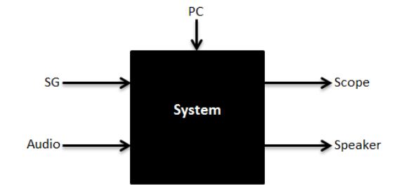
Figure 1 . System Blackbox Diagram
Figure 1 shows a blackbox diagram of the DSP system under design. Inputs to the Nexys2 consist of either the signal generator (SG) or an audio signal provided by a stereo sound source from a computer, iPod, or cell phone. Monitoring the filtered output signal will incorporate an oscilloscope or a stereo speaker connected with the Digilent PmodCON4 RCA audio jack, for the SG and Audio inputs respectively. Programming the Nexys2 will require a USB connected PC and Digilent’s Adept Software.
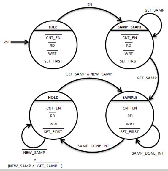
Figure 5. SAMPLE_CTRL.vhd State Transition Diagram
The sampling timing control module controls timing for ADC input and begins DAC output of filtered signals. It also handles storing and delaying input samples and filtered output signals through the single-in parallel-out (SIPO) shift register module SIPO_SHR.vhd. The module contains one small FSM, shown in Figure 5, which determines timing for the RD_EN and WRT_EN signals that determine ADC and DAC operation.
VHDL IMPLEMENTATION

Figure 33. SAMPLE_CTRL.vhd Behavioral Simulation–Verification of CS and SYNC
Because of their dependence on each other, SAMPLE_CTRL.vhd and CONVERTER_CTRL.vhd were simulated and tested together. Figure 33 shows a behavioral simulation using the testbench found in Appendix D. These results verify tog gling action of the ADC chip select signal CS and the DAC chip select signal SYNC. As shown in the results, CS is brought high on the rising edge of the sampling clock signal SAM P_CLK. The SAMP_DONE flag cues the completion of sample acquisition, toggling SYNC to begin output through the DAC.
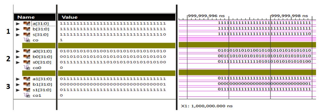
Figure 35. RC_ADDER_32BIT.vhd Behavioral Simulation
Figure 35 displays a behavioral simulation of the RC adder module. The results display sums from 3 different test cases. Case 1 shows addition of 2 negative numbers, case 3 shows correction by the overflow circuit, and in case 3 most the adders that make up the RC adder architecture generate carries. The add er gives the correct result for each case. Behavioral simulations performed for each adder module produced identical results.
NEXYS2 IMPLEMENTATION
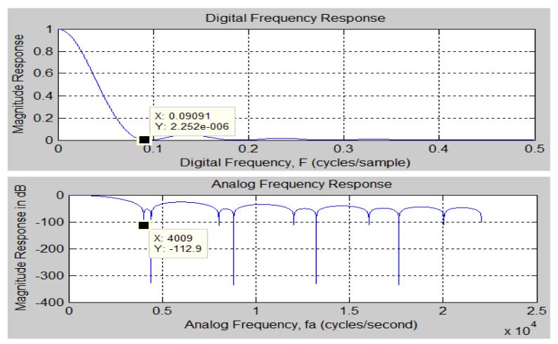
Figure 45 . NORMAL.vhd Test Case 1 Frequency Response Plot from MATLAB
The frequency response of this filter created with MATLAB, displayed in Figure 45, shows that the first zero of the weighted moving average filter occurs at a digital frequency of about .1 cycles per sample. For a 44.1 kHz sampling rate, this is an analog frequency of about 4 kHz.
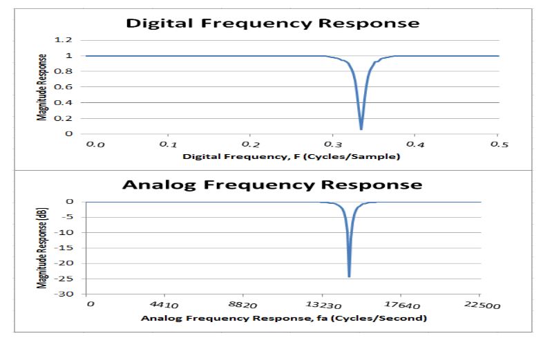
Figure 49 . NORMAL.vhd Test Case 2 Frequency Response Plot from Experimental Data
Figure 49 contains a frequency response plot generated with experimental data from the oscilloscope. It is very similar to the MATLAB generated plot for this test case. The parallel calculation implementation for this test case gave identical results.
DSP PERFORMANCE ANALYSIS
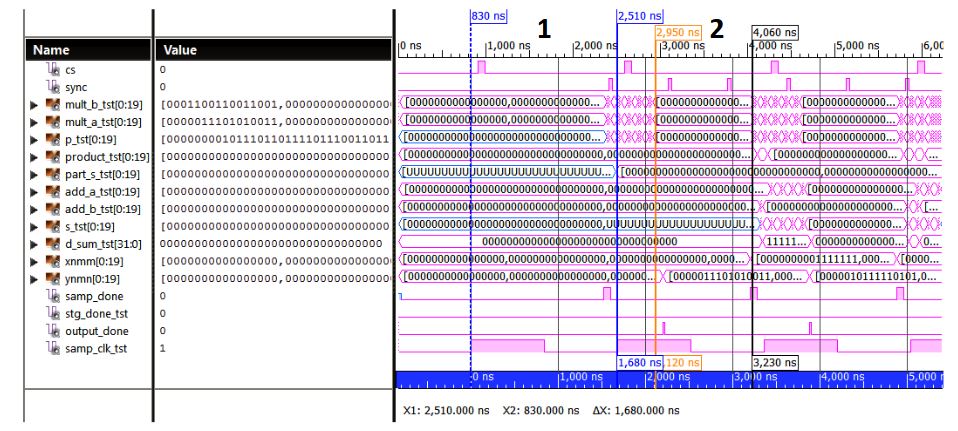
Figure 59. Estimated Maximum Sampling Rate for NORMAL.vhd Serial Calculation Implementation
Figure 59 shows a behavioral simulation for the estimation of maximum sampling rate of the complete system using the NORMAL.vhd module and serial calculations. As seen in the figure, sample acquisition begins on the rising edge of SAMP_CLK and filter calculations begin short after, after the assertion of SAMP_DONE. The way the NORMAL.vhd FSM is constructed, once filter calculations begin they do no stop until complete, even if the ADC begins a new sample.
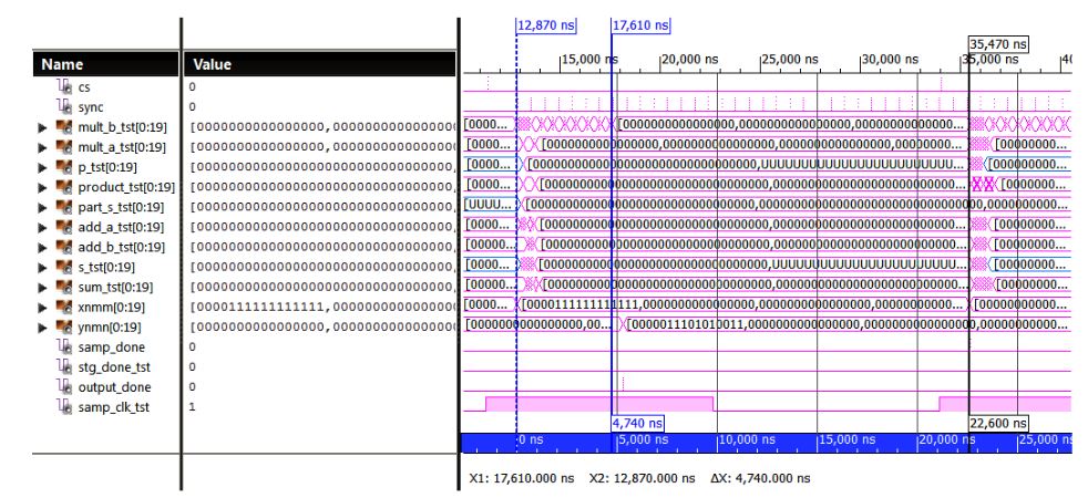
Figure 61. Estimated Maximum Filter Stages for CASCADE.vhd with 44.1 kHz Sampling Frequency
Figure 61 shows a behavioral simulation for CASCADE.vhd using a serial calculation implementation and 9 filter stages. The time it takes to complete the calculation sequence is 4,740 ns and the time in between calculation sequences is 22,600 ns as displayed in the results. With this information the number of filter stages is estimated as about (22,600 / 4,720) * 9 ≈ 43 stages. These results were not verified in the Nexys2 because of the numerous modifications to VHDL modules required to implement a filter of this size.
ARITHMETIC COMPONENT ANALYSIS
This section of the report summarizes information regarding the analysis of arithmetic components designed for the project. It contains comparisons for delay and device resource utilization, and a brief explanation of power analysis. Table 15 contains a summary of analysis performed on arithmetic component architecture. It contains gate delay estimations acquired from the adders schematics and partial product analysis acquired from multiplier algorithms. It also summarizes propagation delay times gathered from timing simulations.
CONCLUSIONS
Binary arithmetic components have expected characteristics, with the larger, more complex components using more system resources and having faster propagation times. However, architecture has little effect on DSP performance when used in the filter realization structures created for Nexys2 implementation. This is despite the fact that each has a different architecture and a different propagation delay. This is because each can calculate its respective output in less than 20 ns, the period of the 50 Mhz Nexys2 system clock.
If a system with a faster clock is used for implementation, component architecture would have more drastic effects on performance. Not all filter realization structures used in the final design functioned properly. The cascade direct form II module, CASCADE.vhd, would produce no output for parallel calculation implementation or for multi-stage filters using serial calculation implementation. This is most likely due to an overflow error in the VHDL code for this module. The normal direct form II module, NORMAL.vhd, seemed to work excellently in all cases.
The audio conversion interface used for the Nexys2 could also use some improvements. The level shifter circuit placed on the input did a good job of providing a clean input signal with an offset of 1.5 V. The output capacitor was able to remove this offset before the signal is sent to the listening device, but introduces a small amount of noise. A better solution may be another level shifter to drop the voltage back to balance around 0 V.
Source: University of Wisconsin
Author: Joseph Waddell
>> 50+ Matlab projects for Digital Image Processing for Final Year Students
>> More Matlab Projects on Video Processing for Final Year Students
>> More Matlab Projects on Audio Processing for Final Year Students
>> More Matlab Projects on Signals and Systems for Final Year Students
>> 200+ Matlab Projects for Control System for Final Year Students
>> 80+ Matlab Projects based on Power Electronics for Engineering Students