ABSTRACT
A basic premise behind modern secure computation is the demand for lightweight cryptographic primitives, like identifier or key generator. From a circuit perspective, the development of cryptographic modules has also been driven by the aggressive scalability of complementary metal-oxide-semiconductor (CMOS) technology. While advancing into nanometer regime, one significant characteristic of today’s CMOS design is the random nature of process variability, which limits the nominal circuit design. With the continuous scaling of CMOS technology, instead of mitigating the physical variability, leveraging such properties becomes a promising way. One of the famous products adhering to this double-edged sword philosophy is the Physically Unclonable Functions (PUFs), which extract secret keys from uncontrollable manufacturing variabilities on integrated circuits (ICs). However, since PUFs take advantage of microscopic process variations, thus many specialized issues including variability, modeling attacks and noise sensitivity need to be considered and addressed.
In this dissertation, we present our recent work on PUF based secure computation from three aspects: variability, modeling and noise sensitivity, which are deemed the foundations of our study. Moreover, we found that the three factors coordinate with each other in our study, for example, the modeling technique can be utilized to improve the unsatisfied reliability caused by noise sensitivity, quantifying the variability can effectively eliminate the impact from noise, and modeling can help with characterizing the physical variability precisely.
RELIABLE PHYSICAL UNCLONABLE FUNCTIONS USING DATA RETENTION VOLTAGE OF SRAM CELLS
The target platform for DRV fingerprinting is an integrated SRAM block with an adjustable supply voltage, as is sometimes used to compensate for variation.To simplify experiments, our platform mimics this configuration using a dedicated SRAM chip and a separate microcontroller. Figure 2.2 presents the overview of our experimental system. SRAM supply voltages are generated using analog outputs of a Texas Instruments MSP430 F2618 microcontroller, and that same microcontroller also orchestrates the timing of the supply voltage changes (per Proc.1). An op-amp configured as a voltage follower tracks the analog output voltage from the microcontroller and powers the SRAM at the same voltage; the op-amp is used because the analog output of the microcontroller cannot supply enough current to power the SRAM directly.
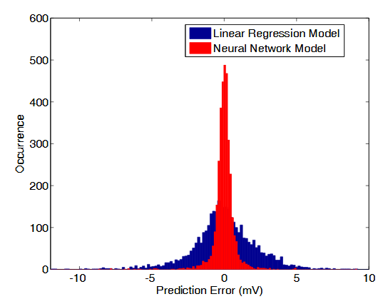
Figure 2.7: DRV prediction error for the artificial neural network model and linear regression model
In both cases, error is determined by comparison to SPICE simulated results. Fig.2.7 presents the prediction error of these models. The neural network model achieves smaller prediction errors than the linear regression model. The mean μ and standard deviation σ of prediction error for the neural network model are − 0.01 mV and 0.35 mV respectively, while those of the linear regression model are 0.041 mV and 0.9 mV.
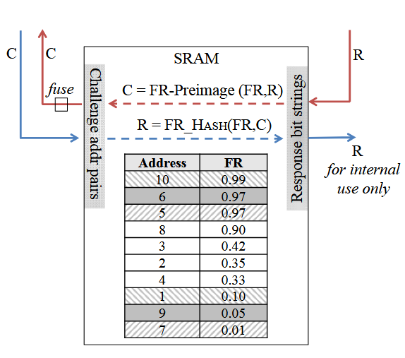
Figure 2.9: Example of DRV-hashing
According to the depicted DRV assignment D, and letting challenge C be (〈 1,10 ,〈 6,9 〉,〈7 , 5 〉), procedure DH (D,C) produces response R = (1,0,1). Similarly, procedure DH-Preimage (D,R), given this response R, would produce as output the same challenge C.
A demonstration of the DRV-based hashing is given in Fig.2.9. According to the depicted DRV assignment D, procedure DH hashes challenge C = (〈 1 , 10 〉,〈 6 , 9 〉, 〈 7 , 5 〉) to response R = (1,0,1): the first response bit is 1 because address 10 has a higher DRV than address 1, the second response bit is 0 because address 6 has a higher DRV than address 9, and the third response bit is 1 because address 5 has a higher DRV than address 7.
RELIABLE PUF DESIGN USING FAILURE PATTERNS FROM TIME-CONTROLLED POWER GATING
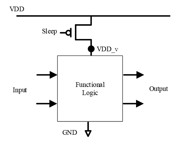
Figure 3.1: Schematic of power gating using a header switch
A PMOS transistor is employed between the supply node (VDD) and the virtual supply node (VDDV) that directly powers the block. A sleep signal enables and disables the connection between VDD and VDDV.
Power gating is an energy-saving technique for embedded systems in which the power supply is effectively turned off for inactive parts of the chip. Power gating is common in modern embedded systems, including the Xilinx 7 series FPGAs, and the ARM Cortex-M series processors. An example schematic of power-gated logic is depicted in Fig.3.1; a PMOS transistor is inserted between the normal supply voltage ( VDD) and a virtual supply voltage (VDDV) that directly powers the logic.
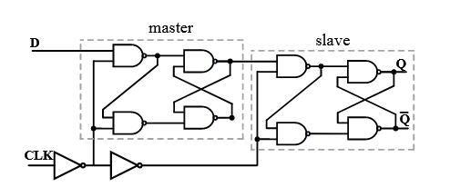
Figure 3.2: Schematic of a positive-edge triggered master-slave D flip flop
Q and ̄ Q are the complementary state nodes that store a single bit value between cross coupled NAND gates. The input value D is stored in the master latch when CLK rises. Nearly simultaneously, the slave latch opens to allow the stored signal from the master to propagate through the slave to the output.
Our work borrows the idea of DRV from SRAM literature and applies it data retention of DFF cells. A positive-edge-triggered master-slave DFF cell can be constructed from two D latches as depicted in Fig.3.2. Like SRAM, DFF cells can fail to retain data when voltage drops too low.
SECURITY EVALUATION AND ENHANCEMENT OF BISTABLE RING PUFS
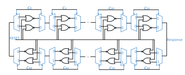
Figure 4.1: Schematic of a single BR-PUF with 64 stages
As depicted in Fig.4.1, a 64-bit BR PUF is composed of 64 stages, where each stage has two inverting delay elements (NOR gates as an example). A challenge vector C = { c1, c2 ,…, cn } selects the NOR gates used in each bistable ring configuration by providing values to the MUX and DEMUX gates of the stages. Since each NOR gate has unique process variation, each different challenge vector creates a unique bistable ring configuration, and in total 224 different configurations can be created.
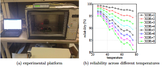
Figure 4.5: Evaluating reliability across different temperatures
Because the reliability of each single BR PUF decreases with temperature, the reliability of the XOR BR PUF results degrade significantly.
Reliability is the ratio of consistent CRPs when a PUF is operating in different environment conditions such as temperature. To evaluate the reliability of XOR BR PUFs, 8 BR PUFs are measured across different temperatures between 270C and 750C, with a 40C step, using a Sun Electronics EC12 Environmental Chamber to control the temperature (Fig.4.5a). Reliability is evaluated by comparing CRPs collected at 270C to CRPs collected at other temperatures.
USING STATISTICAL MODELS TO IMPROVE THE RELIABILITY OF DELAY-BASED PUFS
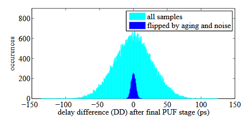
Figure 5.3: Exact delay difference DD of two sets: 50 k golden samples (colored in cyan), the subset of samples flipped by aging and noise (colored in blue).
DDumin ≤ DD ≤ DDumax
For CRP data from Arbiter PUF, DDumax therefore denotes the maximum DD among unreliable challenges, and DDumin denotes the minimum DD among unreliable challenges. If only the challenge vectors that satisfy either DD>DDumax or DD<DDumin are applied to the PUF, then the PUF will be reliable and not prone to flipped response bits. For our simulated 64-bit PUFs based on 45nm Predictive Technology Model (PTM), it is found that DDumax − DDumin = 22.6ps when considering noise, voltage and temperature fluctuations (Fig. 5.3).
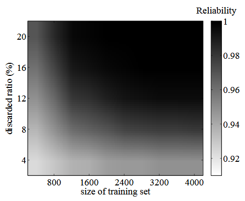
Figure 5.7: Validation under aging and environmental noise, across all of the simulated PUF instances
Trade-off between training size and discarded ratio can be seen in the figure. A larger dr is conservative and can compensate for the lower quality delay predictions of a model trained from a smaller training set.
The qualified challenges ( DDmodel 6∈ [DDmin,DDmax ]) are applied on PUFs, and their responses are compared with golden database, the result is shown as Fig.5.7. With training size increasing, the values learned for DDmin and DDmax become more accurate, and fewer challenges need to be discarded to achieve the same reliability. The runtime to train the SVM model is modest; when using a training set of 4000 CRPs, training takes only 0.38 seconds.
A CLOCKLESS SEQUENTIAL PUF WITH AUTONOMOUS MAJORITY VOTING
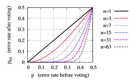
Figure 6.1: The impact of majority voting on reliability of a single bit
For any probability p of an output error in a single trial, p bit is the corresponding probability of having an output error after using majority voting across n trials. Increasing n decreases the probability of error, except for cells with p equal to 0.5.
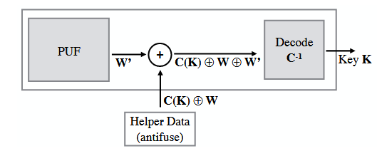
Figure 6.2: PUF-based secret key generation using helper data for error correction
The helper data is generated during a one-time enrollment process and is fixed over the life of the PUF.
Reliability enhancements such as majority voting are complementary to the use of error correction. An example of error correction using the code-offset construction is shown in Fig.6.2. An arbitrary secret key K is chosen for each PUF at enrollment and then encoded to a codeword C (K) that is XORed with PUF response W to generate helper data.
CONCLUSIONS
Driven by Moore’s law, semiconductor industry has experienced continuous physical scaling in the past few decades. This advancement greatly facilitates the development of electronic devices like smart phones, tablets, but also proposes new challenges for hardware security researchers. This dissertation presents some of our recent work in advancing secure CMOS computation with intrinsic functions: i.e., the so-called Physical Unclonable Functions (PUFs). Three topics are studied: nanometer-scale process variations, Machine Learning based modeling and noise sensitivity.
Chapter 1 of this dissertation lists the challenge and opportunities in nanometer cryptographic circuit design. We predict that though process variations are detrimental to conventional circuit design, PUFs have been proposed as a viable solution to harness the unpredictable nature of process variations for security applications. Terminologies like challenge-response pairs (CRPs), reliability, uniqueness and uniformity are defined in this chapter.
Since PUFs leverage microscopic process variations, thus are sensitive to environmental noise like slight temperature or supply voltage fluctuations. Due to such sensitivity, a PUF may not produce consistent response for the same challenge under different environmental conditions. To address the reliability of currently proposed PUF primitives, two highly reliable PUF mechanisms on two common seen memory architectures, SRAM and D Flip-flop are proposed in Chapter 2 and 3. To improve the efficiency of our propose PUF mechanisms, we combined algorithm like binary search, advanced Machine Learning method like Artificial Neural Network (ANN) in these two works.
Source: University of Massachusetts
Author: Xiaolin Xu
