ABSTRACT
Power consumption plays an important role in computer system design today. On chip memory structures such as multi level cache make up a significant proportion of total power consumption of CPU or Application Specific Integrated Circuit (AISC) chip, especially for memory – intensive application, such as floating – point computation and machine learning algorithm. Therefore, there is a clear motivation to reduce power consumption of these memory structures that are mostly consisting of Static Random Access Memory (SRAM) blocks. In this defense, I will present the framework of a novel dual – supply – voltage scheme that uses separate voltage levels for memory read and write operations.
By quantitatively analyzing the cache trace for SPEC2000, Parsec, and Cortexsuite benchmarks and comparing the Read/Write sequence characterization of different computing application types, I discover that memory intensive applications have high potential to generate long consecutive Read/Write sequences, which can be leveraged by our proposed dual supply framework. I then perform a limit study based on ideal Read/Write reordering to obtain the maximum possible power saving estimate. Finally, as a case study, I apply this framework to a custom machine learning ASIC accelerator design to showcase its viability.
BACKGROUND
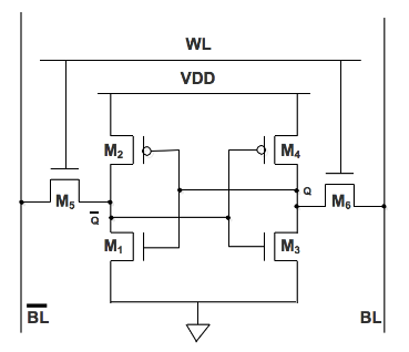
Figure 2.1 6T SRAM
SRAM can retain its stored information as long as power is supplied. The structure of a 6-T SRAM cell, storing one bit of information, can be seen in Figure 2.1. The core of the cell is formed by two CMOS inverters, where the output potential of each inverter Vout is fed as input into the other Vin. This feedback loop stabilizes the inverters to their respective state. The access transistors and the word and bit lines, Word line (WL) and Bit line (BL), are used to read and write from or to the cell. In standby mode the word line is low, turning the access transistors off.
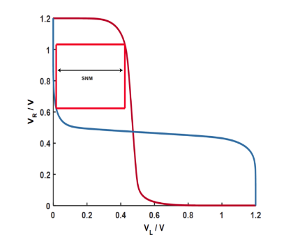
Figure 2.2 SNM
Static Noise Margin (SNM) is an important evaluation of the SRAM cell stability. It can be extracted by nesting the largest possible square in the two voltage transfer curves (VTC) of the involved CMOS inverters, as seen in Figure 2.2. In this figure, VR means the voltage of the right transistor M6 and VL means voltage of the left transistor M5.
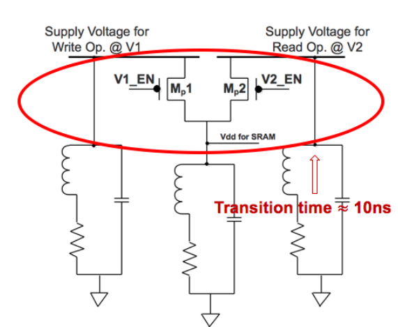
Figure 2.7 Core – level fast voltage switching circuit
In order to separate the voltage supply for read and write operations respectively, we refer the core – level fast voltage switching circuit shown in Figure 2.7 from Booster As Figure 2.7 shows, if V1_EN is set to 1 and V2_EN is set to 0, then Mp1 ON and Mp2 OFF, the VDD for SRAM switch to supply voltage for write operation @ V1. On the contrary, if V1_EN is set to 0 and V2_EN is set to 1, then Mp1 OFF and Mp2 ON, then VDD for SRAM switch to supply voltage for read operatio n@V2.
LIMIT STUDY
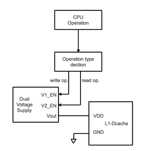
Figure 3.1 Dual supply voltages aggressively switch scheme
The Ideal Case is that we assume that Booster core level fast voltage switching circuit will cost nothing. So that we aggressively switch the dual voltage supply to V1 once there is a single write operation and then switch it to V2 once there is a single read operation, as Figure 3.1 shows.
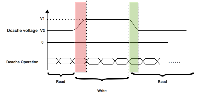
Figure 3.3 Delay penalty analysis
When there is a write operation, which is shown in Figure 3.3 red zone. The dual supply voltages switch from V2 to V1. But there is a nearly 10ns delay each switch from V2 to V1. Before the supply voltage reached V1, the write operation has to stand by since the voltage range from V2 to V1 is not reliable for write operation. So that there is delay penalty when the dual supply voltages switch from V2 to V1.
However, when there comes a read operation that is shown in Figure 3.3 green zone. The dual supply voltages will switch from V1 to V2. In this voltage range from V1 to V2 it is always reliable for read operation. Hence, the read operation does not have to stand by when the dual supply voltages switch. There is no delay penalty when dual supply voltages switch from V1 to V2.
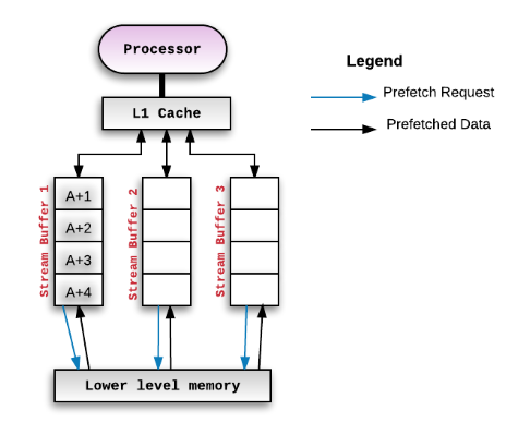
Figure 3.8 Cache prefetching stream buffers
In Figure 3.8, there are several stream buffers between L1 cache and lower level memory. The main purpose of this structure is to address the memory access latency. Since the stream buffers will prefetch the data that maybe used in the near future. It seems that it could help us to predict the near future read and write operation. However, the data in the stream buffer is not the exactly data that will be firmly used to be accessed by L1 cache.
WRITE AGGREGATION BUFFER
In order to reduce the L1-Dcache access times and generate long consecutive read sequence, we propose a Write Aggregation Buffer as Figure 4.1 shows This write aggregation buffer will group the several write operations together, try to prevent the write operation interrupting the long consecutive read sequence.
And It can reduce the read and write total accesses because of Read Bypass and same address Write data self update mechanism. Also, this write aggregation buffer structure will provide the dual supply voltages switches with control logic. From the Figure 4.1, we can conclude that how the write aggregation buffer, dual supply voltages switch L1-Dcache, L1-Icache and processor are integrated together.
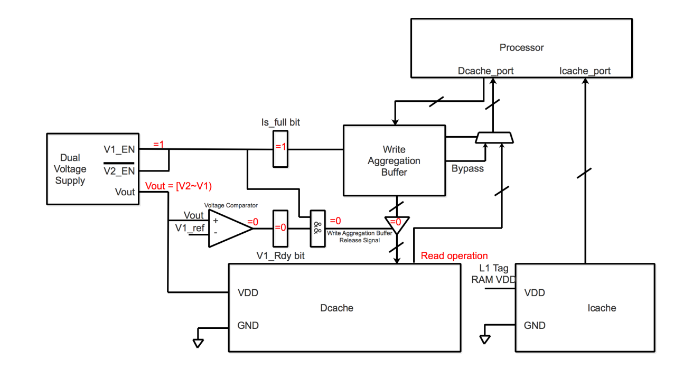
Figure 4.3 Values/status of each register or component of write aggregation buffer structure in red zone time slot
For the red zone time slot, the values/status of each register and component in write aggregation buffer structure are shown in Figure 4.3. W hen the write aggregation buffer is full up, the Is_full bit is set to 1, then V1_EN is set to 1, and dual supply voltages switches switch the voltage from V2 to V1. However, there exists about 10ns delay when Vout goes up from V2 to V1. The red zone indicates the time slot that Vout hasn’t reached to V1. In this time slot, V1_Rdy is always reset to 0.
Because there is a voltage comparator that compare Vout with V1, If Vout =! V1, V1_Rdy bit is reset to 0. So that in the red zone time slot, the access is still read operation since V1_Rdy bit is always set to 0 and then write aggregation buffer release signal is always set to 0 that make write operation cannot happen at that time slot. And the voltage range from V2 to V1 is still reliable for read ope ration. Therefore, L1-Dcache does not have to stand by to wait Vout reach to V1, there is no delay penalty here.
CASE STUDY
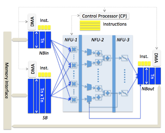
Figure 5.1 DianNao accelerator architecture
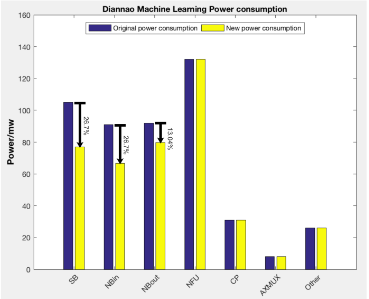
Figure 5.2 Approximate power saving using dual supply voltages in DianNao accelerator
Figure 5.1 shows the architecture of DianNao accelerator. Combine the architecture of this accelerator, the dataset they used for this machine learning accelerator and the control instruction table. We can approximate the power saving shown in Figure 5.2 of SB, NBin and NBout using dual supply voltages. SB save about 26.7% power, NBin reduce the power about 26.7 and NBout slightly reduce the power by 13.04%. Because NBout are used for the buffer to save the intermediate result of this machine learning network.
FUTURE WORK
The write aggregation buffer is similar to store queue in CPU and is also very similar to store buffer in Intel Haswell Arch. So that we would like to merge them together to reduce the additional power consuming. Because build a new buffer architecture is a kind of trade off. When we build a new component, it will bring other power cost, such as the combinational logic power consuming. Therefore, merging design should be a best way to balance this problem.
Secondly, our write aggregation buffer will break the spatial locality in some way. But it is a kind of trade off between power and performance. We plan to replay the new cache trace with write aggregation buffer to gem5 replay interface and analyze how those parameters will be impacted if we use this kind of write aggregation. Finally, we are still expecting that find some solid clue to predict read and write sequence. Maybe it is not an easy work. However, if we reach to this destination, we will have more opportunity to reduce the power using dual supply voltages.
CONCLUSIONS
In this thesis, we reduce the Cache power consumption using dual power supply, which makes Caches works at lower voltages in read status and works at high voltage in write status. We use gem5 and McPAT to analyze the leakage and dynamic power breakdown for CPU, and conclude that cache consume a large part of total power consumption.
We use gem5 to do the cache trace of L1Dcache based on different type benchmarks. Conclude that different benchmarks have different cache trace characterization. Machine learning benchmarks are usually memory intensive application and SPEC2000 are the computation intensive.
We propose write aggregation buffer to group the write operations together, in order to generate long consecutive read sequence, which will increase the power reduction opportunity using dual voltage supply. We do case study to learn that dual voltage supply should reduce the power consumption of SRAM in ASIC chip more efficiently.
Source: Washington University
Author: Gu Yunfei
