ABSTRACT
Two-dimensional van der Waals materials have been a subject of intense research interest in recent years. High thermal conductivity of graphene can be utilized for many thermal management applications. In spite of possessing very high electron mobility, graphene can’t be used as transistors because of the absence of band gap; however transition metal dichalcogenides are another class of two-dimensional van der Waals materials with inherent band gap and show a great promise for future nanoelectronic applications.
But in order to tailor these properties for commercial applications, we should develop a better understanding of the effect of extrinsic factors like size, rough edges, grain boundaries, mass-impurities, interaction with substrate etc. on thermal and electrical transport.
Most materials exhibit a smooth ballistic-to-diffusive type of thermal transport in which when the sample size is small as compared to mean-free-path of phonons the transport is ballistic, whereas, when the sample size is large as compared to phonon mean-free-path, phonons undergo multiple scattering events and the thermal transport becomes diffusive in nature.
However, graphene exhibits an atypical thermal transport behavior where thermal conductivity shows an increasing logarithmic trend even for samples far greater than the mean-free-path of phonons. We show that this anomalous behavior can be attributed to the significant contribution coming from momentum-conserving normal phonon-phonon scattering. Secondly, graphene grain boundaries have been found to significantly reduce thermal conductivity even in the presence of substrates.
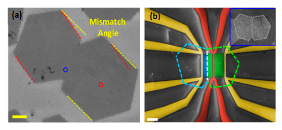
In spite of numerous studies on the effect of grain boundaries (GBs) on thermal conductivity in graphene, there lacks a complete correlation between GB resistance and misorientation angle across graphene GBs.We show a direct correlation between thermal GB resistance and mismatch angles with low angle mismatch can be captured only by GB roughness, whereas, large mismatch angles will lead to the formation of a disordered patch at the interface and it could significantly deteriorate the overall thermal conductivity even in the presence of substrates.
GBs are found to affect electrical transport in two-dimensional systems as well. Owing to the excellent electronic properties and compactness of these two-dimensional materials, high quality 2D heterojunctions are the subject of intense research interest in recent years. Graphene-MoS 2 heterojuctions are found to form ohmic contacts and show great potential for future nanoelectronic applications.
We show that the interface resistance in Gr-MoS 2 heterojuctions can affect the overall resistance of the device if the channel (MoS 2) length is small at low carrier densities, whereas, at high carrier densities interface resistance do not play much role in determining the resistance of the entire device.
However, if graphene and MoS 2 grains are misorientated then interface resistance can play a crucial role in determining the overall resistance of the device. We also show a weak dependence of misorientation angles on GB resistance across MoS 2 grain boundaries.
SIZE DEPENDENCE OF THERMAL CONDUCTIVITY IN GRAPHENE NANORIBBONS
Theoretical Calculations Using Improved Callaway Model:
Several techniques have been employed to model thermal transport in graphene such as non-equilibrium molecular dynamics (NEMD), non-equilibrium Green’s functions (NEGF) and Boltzmann transport equation simulations. In our work, we have used the solution of full phonon Boltzmann transport equation (pBTE) in order to calculate thermal conductivity in GNRs based on Allen’s improved Callaway model.
Results and Discussion:
The size dependence of thermal conductivity in GNRs has been studied under two separate headings in this work (a) Length dependence (b) width dependence of thermal conductivity.
Length dependence of thermal conductivity
To study length dependence of thermal conductivity at room temperature, we scaled ribbon length while keeping the width constant (W=1.5μm) in order to mimic the experimental set-up by Xu et al. In thermal conductivity of free-standing graphene has been plotted against length for various discretization densities of the phonon dispersions.
The red curve shows a convergence in thermal conductivity for a coarse discretization of q-points having 100,000 points in the first Brillouin zone. Previous studies suggest that a major part of thermal conductivity comes from the quadratic out-of-plane ZA modes and divergence is a consequence of long wavelength problem. Klemens was among the first to propose a logarithmic divergence of thermal conductivity in the two-dimensional phonon gas.
Width dependence of thermal conductivity
Next we turn to the width dependence of thermal conductivity in suspended graphene ribbons at room temperature and vary the width W while keeping L = 10 μ m and a constant edge roughness ∆=2 nm, which puts the ribbons in the fully diffusive edge scattering regime. It can be seen that the resistive part of thermal conductivity (KC) shows a gradual width dependence.
EFFECT OF GRAIN MISMATCH ANGLE ON THERMAL CONDUCTIVITY IN CVD-GROWN GRAPHENE
Introduction:
As discussed in chapter 1, thermal management in nanoelectronic devices is one of the major problems faced by the present semiconductor industry to achieve further miniaturization of transistors. 2-D materials have shown a great potential for future electron-ics devices due to their high electronic and thermal properties. Graphene has served as a model 2D system for more than a decade now. Large-scale manufacture of graphene for commercial purposes are mostly done by chemical-vapor deposition (CVD) technique.

(a) Shows Scanning Electron Microscopy (Sem) Image of Two Merged Hexagonally Shaped Single Crystalline Graphene Grains Forming an Individually Grain Boundary (Gb). The Scale Bar Is 5 Μm. (B) High-magnification Image of a Fabricated Thermometry Platform Comprised of a Heater Electrode in the Center and Two Sensor Electrodes on the Sides Having Perfect Symmetry. The Scale Bar Is 5 Μm.
Theoretical Modelling of Thermal Transport Across Graphene Gb:
The primary carriers of heat in graphene are phonons. Fourth nearest neighbor force constant model, as described by Saito, has been used to calculate phonon dispersion. Phonon dispersion of an isolated sheet has been considered for this study, which is a good approximation. The model used for this study is based on the complete solution of phonon Boltzmann transport equation (pBTE) same as used in Chapter 2 and is given by the eqn. 2.1.
EFFECT OF GRAIN BOUNDARIES IN TWO-DIMENSIONAL LATERAL GRAPHENE-CONTACTED MOS2 HETEROSTRUCTURES
Theoretical Modeling:
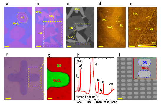
To shed light on the origin of the improved electrical performance of the graphene contacted MoS 2 devices, the individual electronic band structures of graphene and MoS 2 was calculated using first-principle Density Functional Theory as implemented within the open-source distribution Quantum-Espresso.
The total resistance (Rtot) of the whole device between source and drain is comprised of the series resistances from the graphene grains (Rgrap, forming source and drain), resistance of MoS2grain (RMoS2), constituting the channel) and resistances from the grain boundaries (RGB) formed at the interface between graphene and MoS2.
Results:
On applying gate voltage, but before any source-drain bias is applied, the Fermi levels in both graphene and MoS 2 away from the interface shift relative to their position at zero gate voltage in response to the induced charge in the 2-dimensional layers.
Consequently, the energy bands on both sides of interface rearrange themselves to maintain the equilibrium condition. However, the shift in the bands on the two sides is not identical because the two materials have different densities of states, leading to an increase in band bending in the MoS2 with increasing gate bias.
IMPACT OF MISMATCH ANGLES ON ELECTRONIC GRAIN BOUNDARY/INTERFACE RESISTANCE IN LATERAL TWO-DIMENSIONAL HETEROSTRUCTURE
Theoretical Approach:
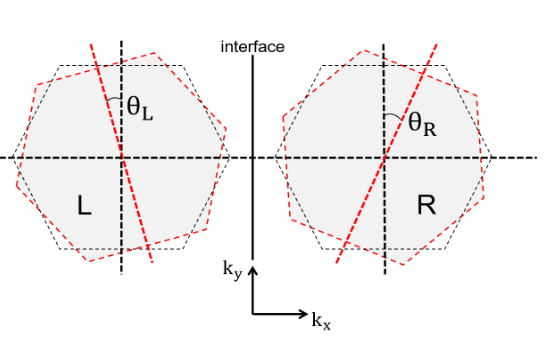
In our numerical model we calculate the electronic bandstructure for bulk graphene and MoS 2 from first principles. The bands are aligned at the interface using electron affinity model. The effect of grain boundary/interface is incorporated using boundary conditions based on elastic theory.
From translational symmetry, elastic transmission requires simultaneous conservation of energy of the incident electron as well as conservation of its momentum parallel to the interface. Here we assume the interfaces are free from trapped and surface impurities; consequently the bands are assumed to be well-aligned across the interface with same materials on either side.
Results and Discussion:
Before discussing about the impact of mismatch angle between two grains on grain boundary resistance (RGB), we calculated ballistic resistance in graphene-graphene (Gr-Gr)interface and compared it with analytically calculated values.
We define ballistic resistance as the resistance between two perfectly-matched grains i.e. when misorientation angle is 0◦. Let us first discuss about how to calculate ballistic resistance of graphene-graphene interface.
CONCLUSION
In conclusion, we find that misorientation angle between two adjacent grains play a very significant role in both homojunctions and heterojunctions. We show that the grain boundary resistance across graphene GBs vary over a very wide range depending on the degree of mismatch between adjacent grains and type of GBs. Twin GBs are found to scatter electrons rather coherently, whereas tilt GBs strongly affect transmission of electrons across them.
However in comparison with graphene, MoS 2 shows weaker dependence on misorientation angle for both twin and tilt GBs. This can be attributed to the flat parabolic band structure around K-valleys in MoS 2 as compared to the steep linear E-k relationship around K-valleys. We also show that the interface resistance across Class-II graphene-MoS 2 heterojunctions exhibit a strong dependence on misorientation angle, whereas the interface resistance in Class-I graphene-MoS 2 heterojunctions is almost independent of the effect of mismatch angles. However, Class-I interfaces exhibit a strong dependence on carrier densities.
Source: University of Massachusetts
Author: Arnab K. Majee

