ABSTRACT
An intelligent, portable, and high throughput digital microfluidic (DMF) system is developed. Chapter 1 introduces microfluidics and DMF systems. In Chapter 2, a low-cost and highre solution capacitive-to-digital converter integrated circuit is used for droplet position detection. A field-programmable gate array FPGA is used as the integrated logic hub of the system for highly reliable and efficient control of the circuit. In this chapter a fast-fabricating PCB (printed circuit board) substrate microfluidic system is proposed.
Smaller actuation threshold voltages than those previously reported are obtained. Droplets (3 μL) are actuated using 200 V, 500 Hz DC pulses. Droplet positions can be detected and displayed on a PC-based 3D animation in real time. The actuators and the capacitance sensing circuits are implemented on one PCB to reduce the size of the system. In Chapter 3, an intelligent EWOD (electrowetting on dielectric) top plate control system is proposed. The dynamic top plate is controlled by a piezoelectric (PZT) cantilever structure.
A high resolution laser displacement sensor is used to monitor the deflection of the top plate. The gap height optimization and the harmonic vibration significantly improve the droplet velocity and decrease the droplet minimum threshold actuation voltage. The top plate vibration induced actuation improvement is magnitude and frequency dependent. 100 μm and 200 μm vibrations are tested at 25 Hz. Vibration frequencies at 5 Hz, 10 Hz, and 20 Hz are tested while the magnitude is 200 μm. Results show greater improvements are achieved at larger vibration magnitudes and higher vibration frequencies.
With a vibrated top plate, the largest reduction of the actuation voltage is 76 VRMS for a 2.0 μl DI water droplet. The maximum droplet instantaneous velocity is around 9.3 mm/s, which is almost 3 times faster than the droplet velocity without top plate vibration. Liquid that has different hysteresis such as acetonitrile with various concentrations are used as a control to show its compatibility with the proposed DMF chip. Contact line depinning under top plate vibration is observed, which indicates the underlying mechanism for the improvements in actuation velocity and threshold voltage.
The top plate control technique reported in this study makes EWOD DMF chips more reliable for pointof- care diagnostics. In Chapter 4, the mechanisms of the improvements were investigated by observing the detailed changes in the contact angle hysteresis using both parallel and nonparallel top plates. In Chapter 5, on-chip cell cultures are used for anti-biotic resistant bacteria detection. The passively dispensed on-chip cell cultures realize the isolated micro environment electrochemistry measurement, shorten the culturing time, and reduce the required sample volume.
The design of the next generation ultra-portable DMF system is covered in the Appendix. Detailed technical notes and hardware design is covered in the Appendix. The proposed portable and high throughput DMF system with on-chip cell cultures have a great potential to change the standards for micro-environment culturing technologies, which will significantly improve the efficiency of actuation, sensing, and detecting performance of the DMF systems.
PCB DIGITAL MICROFLUIDICS
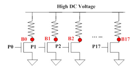
Fig. 2.1 Schematic of the voltage supply circuit.
A high-voltage square wave is created at the drains, B0-B17, of NMOS transistors (VN2460) seen below in Fig. 2.1. P0-P17 are connected to the I/O ports of the microcontroller. For example, if P0 goes high then B0 goes low. If P0 goes low then B0 is pulled to the High DC Voltage through a resistor.
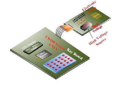
Fig. 2.3 Diagram of the electro-wetting system.
A diagram showing the electrowetting system is seen in Fig. 2.3. The control section of the system is a separate board, with display and keyboard. The electrode array is placed along with the high-voltage supply on its own board. A cable is used to connect the control board to the array board.
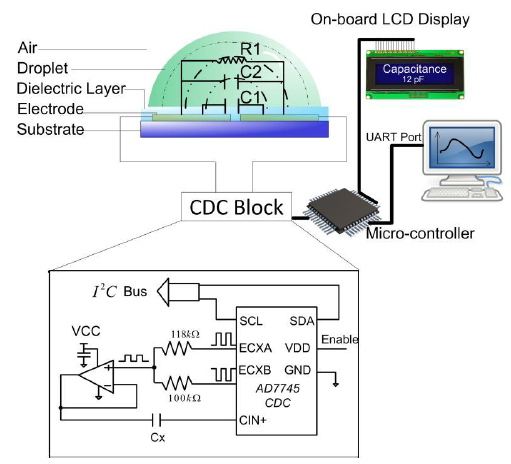
Fig. 2.14 Diagram of the CDC system.
A high resolution capacitance-to-digital converter (CDC) (AD7745, Analog Device, Inc., MA, USA) is used for the front-end capacitance measurement. The AD7745 has a resolution of 24-bits. Without using an extension circuit (in the CDC Block) shown in Fig. 2.14, the CDC’s measurement range is 4 pF. The measurement range can be extended to 48 pF if the extension circuit is applied.
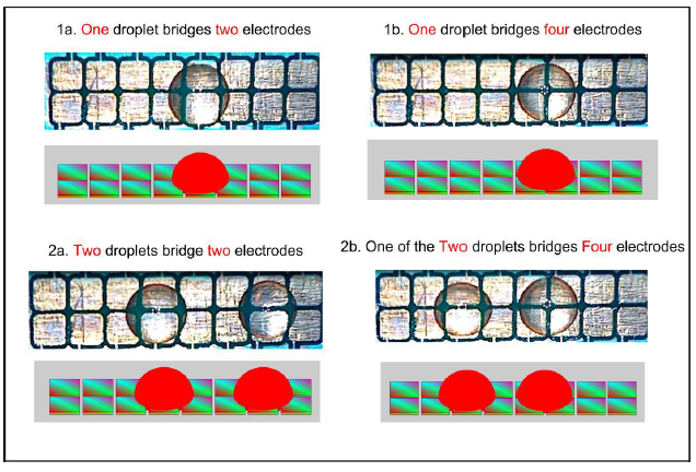
Fig. 2.27 Static droplet position detection in air environment.
Fig. 2.27 Static droplet position detection in air environment for (1a) one droplet bridges two electrodes, (2a) two droplets bridges two electrodes, (1b) one droplet bridges four electrodes, (2b) one of the two droplets bridges four electrodes. The droplets are put on the electrode array by pipette. The system can detect if the electrode is fully occupied, half occupied or ‘off’ the electrode. Single-plate electro-wetting device is used in the system, which means the first row of electrode array shown in this figure is activated by alternative high-voltage pulses, the bottom row of the electrode array is grounded.
GLASS SUBSTRATE DIGITAL MICROFLUIDICS
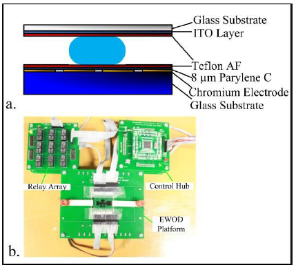
Fig. 3.1 The EWOD chip fabrication layers (a) and the EWOD system (b).
EWOD describes a configuration in which an insulating layer separates the working liquid and actuation electrodes. PCB (printed circuit board) EWOD chips are low cost and easy to fabricate, but the driving voltage is high and oil environment is required for a smooth actuation. A reliable EWOD DMF chip with an 8 μm parylene C dielectric layer is proposed in this study (Fig. 3.1). Droplet dispensing, merging and splitting are tested under various droplet volumes. The droplet dispensing accuracy and splitting minimum voltages are discussed.
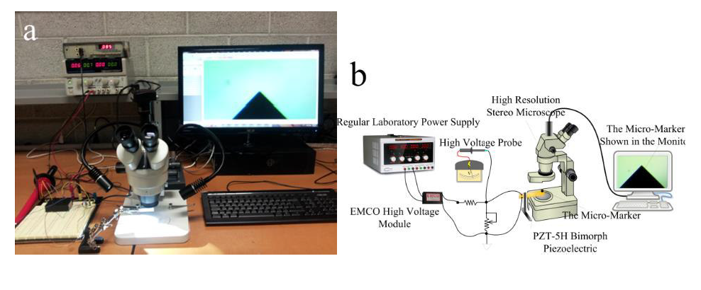
Fig. 3.10 (a) The PZT-5H displacement measurement system. (b) The diagram of the PZT-5H displacement measurement system.
The bimorph piezoelectric actuator (SM 311, PZT-5H) is purchased from Steiner & Martins, INC, which has a maximum actuation of 2 mm with a 200 Hz bandwidth. A regular laboratory power supply is used to trigger the high voltage module (EMCO F40, Schweiz, Switzerland) (Fig. 3.10).
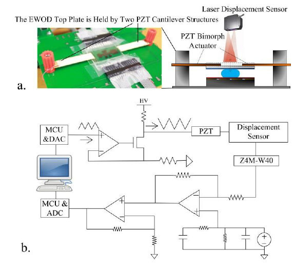
Fig. 3.20 (a) The experiment setup of the EWOD system and the cross section of the PZT cantilever structure with the EWOD system. (b) The proposed portable EWOD top plate positioning system.
A desktop PC (ASUS, Intel i5 2.53 GHz, RAM 8 GB) is used for data collection and sending driving voltages to the DAC & MCU module. The DAC translates the digital driving voltages to 0-2.7 V. An additional linear high voltage amplifier is developed to modulate the 0-2.7 V to 0- 200 V to drive the PZT plates (Fig. 3.20).
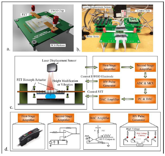
Fig. 3.26 (a and b) The 3D model and the experiment setup of the EWOD platform. (c and d) The system overview of the DMF and the PZT top plate control module.
A novel modular design is introduced to the EWOD system. The EWOD electrode control system is integrated into two portable modules (Fig. 3.26 (b)); one is the relay array, the other one is the control hub. The EWOD chip is mounted on a PCB platform and connected to the relay array module with standard flexible flat cables (FFC). EWOD electrode driving voltages are obtained from the drains of the high-voltage CMOS transistors (Fig. 3.26 (d)).
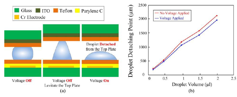
Fig. 3.37 The top plate vibration has limits in amplitude to avoid the droplet detaching from the top plate.
In the regular top plate vibration operations in this study, the gap height and vibration amplitude is much lower than the vibration limit presented in Fig. 3.37. For example, for a 0.5 μl droplet, the detachment happens at > 500 μm, but the largest possible gap height with vibration is 300 μm in our study (limited by the PZT material). High gap height lowers the aspect ratio of the droplet which impacts on the actuation velocity, so there is no motivation for the user to apply “large” vibration amplitude to the top plate.
EWOD DMF CHIP SURFACE CHARACTERIZATION
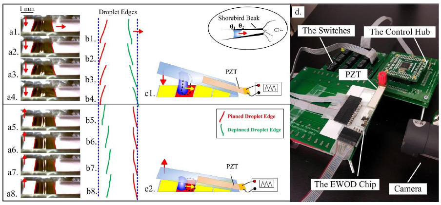
Fig. 4.2 A ratchet-like motion cycle of a 4 μL droplet in a non-parallel EWOD device. (a1-a8) A droplet bounded by a shorebird’s beak and moves into the wedge with non-parallel top plate vibration. (b1-b8) The corresponding left (rear) and right (front) edges of the droplet in a1-a5. (c1 and c2) Illustrations of the EWOD system with non-parallel substrates and the EWOD model to mimic the shorebird beak to bound a droplet. A PZT chip is used to create a beak-like vibration (not drawn to scale). (d) The system setups.
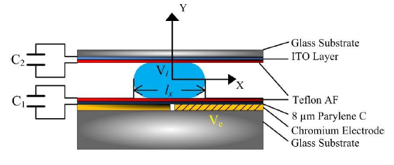
Fig. 4.5 Capacitance and geometrical model of a droplet in EWOD device.
The droplet net force can be represented by the capacitive energy stored in the dielectric material coatings (Baird, Young, & Mohseni, 2007). The capacitance distribution and the geometric structure are modeled in Fig. 4.5.
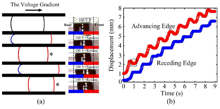
Fig. 4.14 (a) The cross-sectional view of the semi-ratchet-like motion of the advancing and the receding edge of a water droplet. (b) Trajectory of the semi-ratchet-like motion of the advancing and receding edges.
The step size for each ratchet movement is limited by the hysteresis ‘level’ at the front contact line in addition to the vibration magnitude. If AC subthreshold voltage is being used, compressing the droplet hard will push the front contact line further during the compressing regime, but the front contact line will recede back with the rear contact line during the relaxing regime (Fig. 4.14).
ON-CHIP CELL CULTURES FOR ANTI-BIOTIC RESISTANT BACTERIA DETECTION
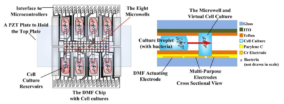
Fig. 5.1. The proposed topology of the DMF chip. The top plate is an ITO coated transparent glass, held by a PZT plate.
Our approach will use digital microfluidics (DMF) electrowetting on dielectric (EWOD) chips to carry out on-chip electrochemistry measurements instead of using magnetic beads and PCR. We passively dispense a micro-liter droplet into the “virtual microwell” (Fig. 5.1) to a hydrophilic area on a DMF chip (Eydelnant, Uddayasankar, Liao, & Wheeler, 2012; Ng et al., 2015). The microwell environment can provide an ultra-low noise isolated culture ambient and enables cyclic voltammetry measurements.
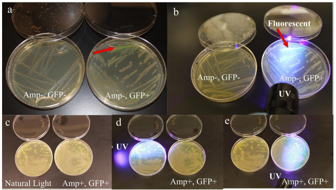
Fig. 5.3 Results of the pGREEN gene transformation.
Fig. 5.3 Results of the pGREEN gene transformation. (a) The Amp-, GFP- petri dish does not have GFP gene, so only regular E. coli strain grows; the Amp-, GFP+ petri dish has GFP gene but does not have antibiotics (Ampicillin), so the regular and the transformed E. coli grow together and compete against each other. Only few GFP transformed E. coli mutant are observed (red arrow). (b) Using a UV light source to observe the fluorescent glow of the transformed E. coli. (c-e) Petri dishes based cultures with antibiotics (ampicillin) added to the culture.
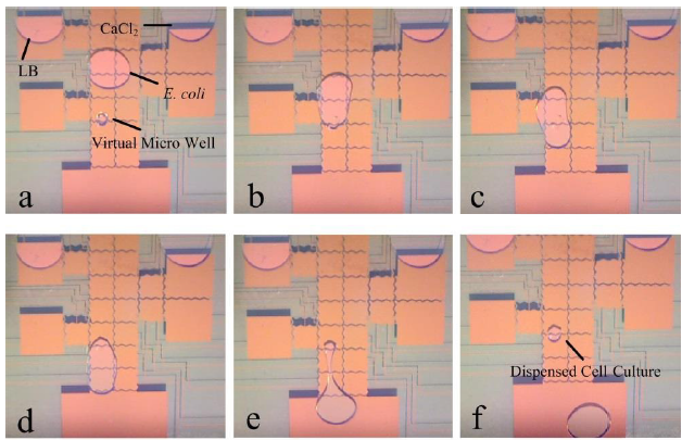
Fig. 5.7 Passively dispensing bacteria cultures.
The most significant advantages of using on-chip cell cultures and micro electrode on-chip electrochemistry measurements are shorter culturing duration and smaller sample volume. Shortening the culturing period can provide accurate diagnostic results at the earliest time for the most efficient treatment; the smaller sample volume can reduce the patients’ stress and pain at the sampling phase. The formation of the on-chip micro cell cultures is demonstrated in Fig. 5.7.
SUMMARY, CONTRIBUTIONS, AND FUTURE WORK
This dissertation covers both low-cost DMF chips on PCB and high performance glass DMF chips; their surfaces are characterized using contact angles (c.a.), c.a. hysteresis, threshold voltages, and actuation velocities. Significant improvements are observed by using the proposed dynamic top plate into the DMF system. A super portable control interface allows users to operate the droplets on any WiFi terminals, such as a smart phone or a laptop, which avoids massive wire connections. Using this developed DMF system for the on-chip bacteria cultures and electrochemistry measurement are promising for bacteria susceptibility detection and other microbiological experiments.
The purpose of my study is to develop a lab-on-chip micro droplet actuator, which can be controlled by a smartphone or a laptop wirelessly through the WiFi connection. The micro droplet actuator is built upon a Chromium coated electrode array on a glass substrate. Superportable 3-D printing chip interfaces connect the chip pads to external control electronics. A highly efficient high-voltage module is developed to provide up to 200 V DC as the driving voltages.
The on-chip oscillator provides 0-10 kHz, 5 V pulses as the MOSFET gate-toggling signal for the generation of the β00 V pulses at the ‘drains’ of the MOSFETS. The digital microfluidic chip developed upon the EWOD technology is called ‘digital microfluidics (DMF)’. By using this technology, the micro-liter level droplets can be manipulated in a high throughput manner, which is promising for the next generation laboratory automation technology. Future applications, such as intelligent DMF with embedded systems, electrowetting optical lenses, adaptive droplet volume control, bio-inspired renewable energy optimization, bio-MEMS, onchip cell cultures, and point-of-care diagnostics will be explored.
Source: University of Nevada
Authors: Yiyan Li
>> 200+ IoT Led Projects for Final Year Students
>> 200+ IoT Led Engineering Projects
>> IoT Projects in Medical Field for Final Year Students
>> IoT Environmental Monitoring System for Smart Cities Projects for Students
>> More Wireless Projects based on Fpga for Final Year Students
